
DIY Double-Sided PCBs w/ Soldermask
Over the years, I’ve tried pretty much every trick in the book to make PCBs at home, but to no avail. It’s brought nothing but frustration and inconsistent results. If all you’re making are boards that use through-hole and large SMD components, feel free to use any method you come across. In my opinion, trying to use as many SMD components as possible is cheaper, smaller, and overall just easier to work with. However, to make routing easier, this necessitates sub-10mil trace and space boards, which means milling is no longer a reliable option. The toner transfer method offers the best balance of cost and effectiveness.
Cost and time are the two big things to consider when deciding to make your own PCBs. If you need same day turnaround or only one copy of a board, it’s economical to make boards yourself. Single sided boards are also good candidates for the DIY route. However in most cases, I’d say it’s best to just the send the board off to a manufacturer if you can wait. Once boards get to above 70mm in size and need sub-8mil trace/space and start needing more vias, I’d say it’s pretty much necessary to let someone else do the manufacturing. Nowadays, including shipping you can get 5 pieces of a 100mm x 100mm 6mil trace/space board for about $25.
Availability and cost of materials are big factors I considered when developing my own style of making PCBs. If it’s too expensive or materials are hard to come by, I’d rather just send the boards off to a manufacturer. I’ve heard of a photoresist method, but in my experience it’s a bit expensive and hard to come by so while I’m certain it works very well, it’s not something I’ve tried yet.
Design Considerations
In my experience, 10mil trace/space boards are really easy to make and are suitable for most projects. 8mil boards are more difficult but with practice I’m getting better and better at them. It’s more of a timing thing than anything. I’ve pushed 6mil before but I honestly haven’t had much experience with those since 8mil is usually good enough.
For vias, the optimal way would be plated through holes but that’s a bit hard. I’ve heard of using PCB rivets which I really want to try one day. The trouble is finding a good cheap source for them. For now, to balance consistency and size, I use 1.5mm outer diameter, 0.5mm inner diameter for vias. Any standard component lead fits perfectly in the 0.5mm hole.
Also, the less copper there is to remove, the faster the whole etching process is later. Still, in the consideration of noise, don’t leave behind copper islands. Anyway onto the actual PCB making process.
PCB Laminator
The problem with the toner transfer method is that people tend to use a clothes iron to do it. That works very poorly and takes a lot of effort. The human factor is a huge source of inconsistency so I desired some way to do toner transfer with as little interference as possible from my end. To that end I built a PCB laminator, which I’ve made a post about. With this tool I can simply put the board in and let it do all the work. Perfect results almost every time.
In all honesty, your PCB laminator doesn’t need to be as complex as mine. Or it could be more complex. To each their own. In fact, some people have gotten this method to work without modifying the laminator at all.
Toner Transfer
The gist of the toner transfer method is to print your PCB design (make sure to mirror it if you need to) onto some paper. Then apply heat and pressure to transfer the toner onto a clean copper clad board. The toner used in laser printers is a polymer with a glass transition temperature of about 132°C, so it’s the temperature to aim for when using this method.
Preparing the Design
To start off we need to get our design onto paper. Everyone always talks about finding the perfect special paper that lets go of the toner so easily. In all honesty, that’s not necessary and just adds cost. I’ve found that standard magazine paper works exceptionally well. Good thing I have an endless stack of Time magazines at home. Since my laser printer doesn’t take too kindly to irregularly shaped, flimsy paper I have to tape it to another sheet of paper before sending it through. If you can, make sure toner density and resolution are at their highest settings.
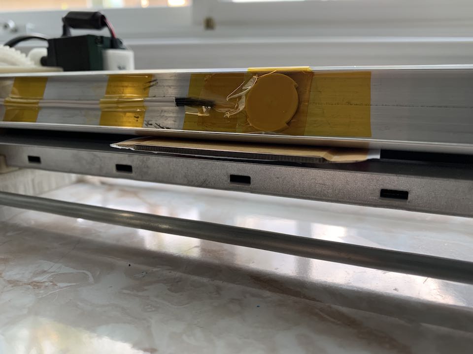
Now cut out your design, making sure to leave some extra on the edges. For a double-sided board, you’re going to need to make a sort of sleeve with the front and back. Alignment of the two sides is pretty critical, so I use a flashlight to make sure all the vias line up.
Prepping the Copper Clad Board
It is crucial that the copper is clean and free of oils or else the toner won’t stick well. I start by using one of those green abrasive dish scrubbers to scuff up the surface of the board. Sometimes I wash the board with soap and water to remove the copper particles. I always follow up with a quick wipe with acetone. Be careful not to touch the copper surface after this.
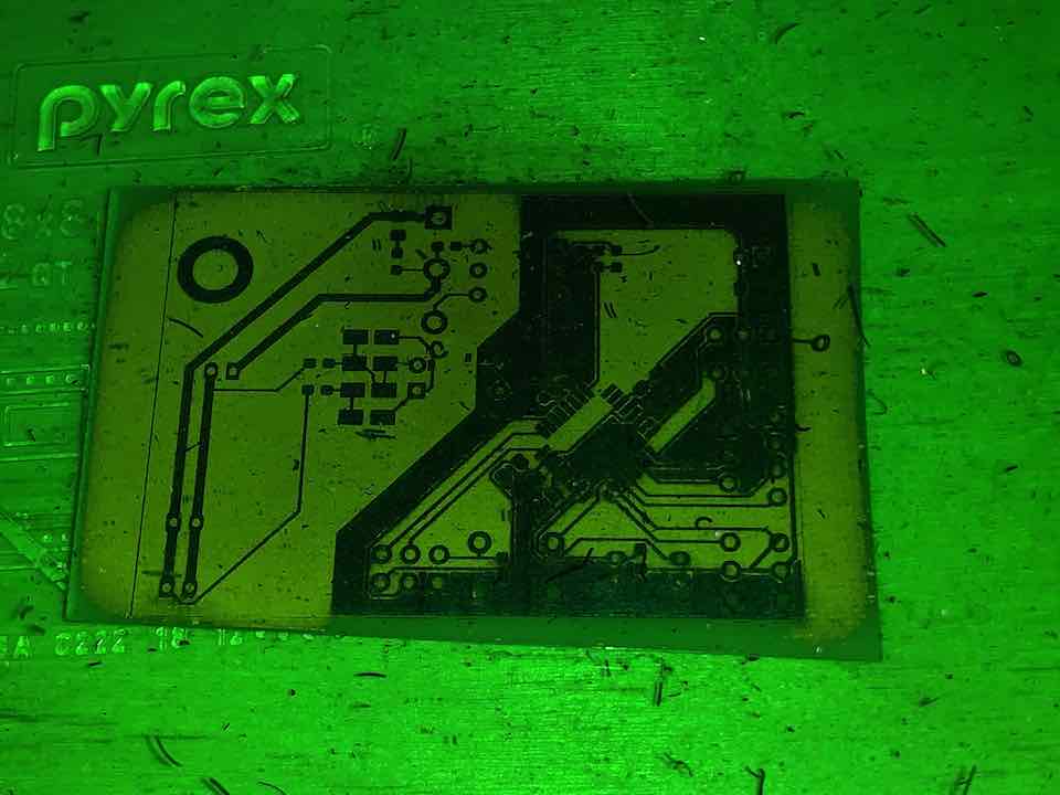
Now slide your copper clad board into your sleeve from earlier, keeping an eye on alignment. It should look something like this.
Removing the Paper
After sending it through the laminator for about 8 minutes, it’s time to remove the paper. I’ve heard of soaking it in soapy water for an hour and then just peeling the paper away, but that takes too long. If the transfer is good, just place the board under running water and peel off the paper. A lot will be left, but a good amount of vigorous rubbing removes the rest of the paper without much damage to the toner. If all goes well, your transfer will look something like this.
I like to use a microscope to double check that toner covers everywhere I need it to.
Etching
Now we’re ready to dunk our board in a vat of acid. The etchant I use is really easy to make and very popular. Just make a 50-50 mixture of muriatic acid (aka pool acid from Home Depot) and off the shelf hydrogen peroxide. This solution lasts pretty much forever and apparently gets stronger with use, although in my experience it gets subjectively weaker. Occasionally, it’s useful to bubble air through the solution to rejuvenate it. To make sure both sides etch at the same time, I tape on little plastic bits to the bottom of the board to elevate it. Dunk the board. Agitating it is useful but I’m lazy so usually I just let the board soak for an hour. I come out every 20 minutes or so to shake the solution around.
It’s a good idea not to leave the container of etchant open since it’s so corrosive. All my tools have a layer of rust now just by placing them overnight near the open container.
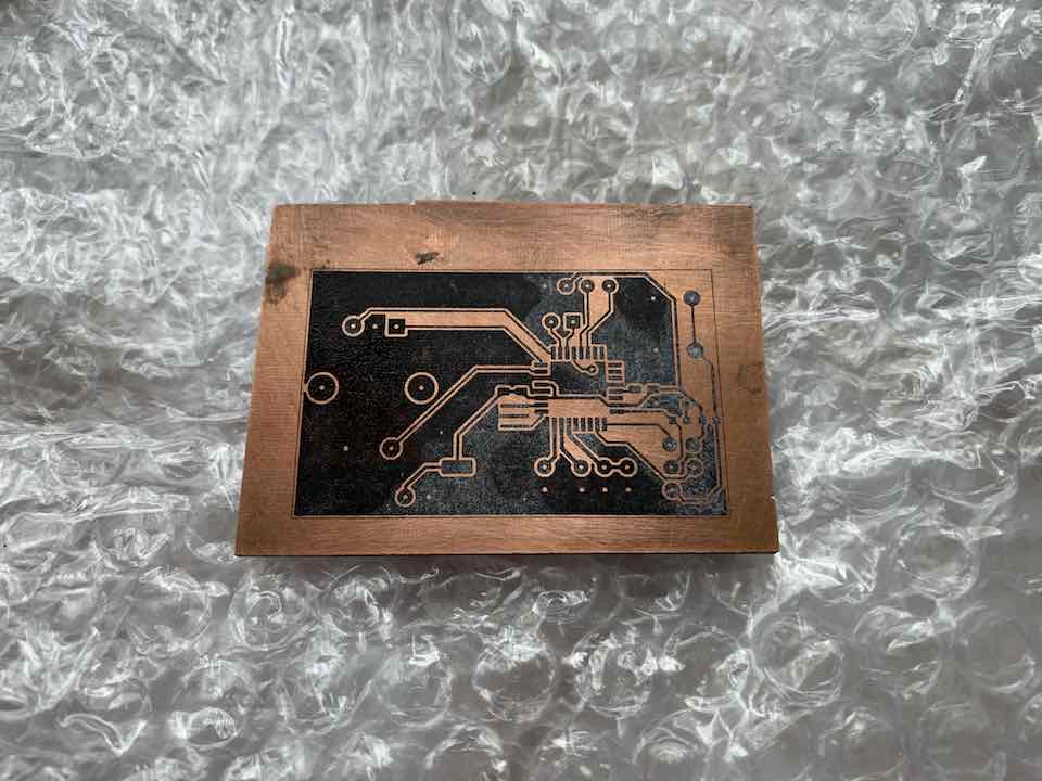
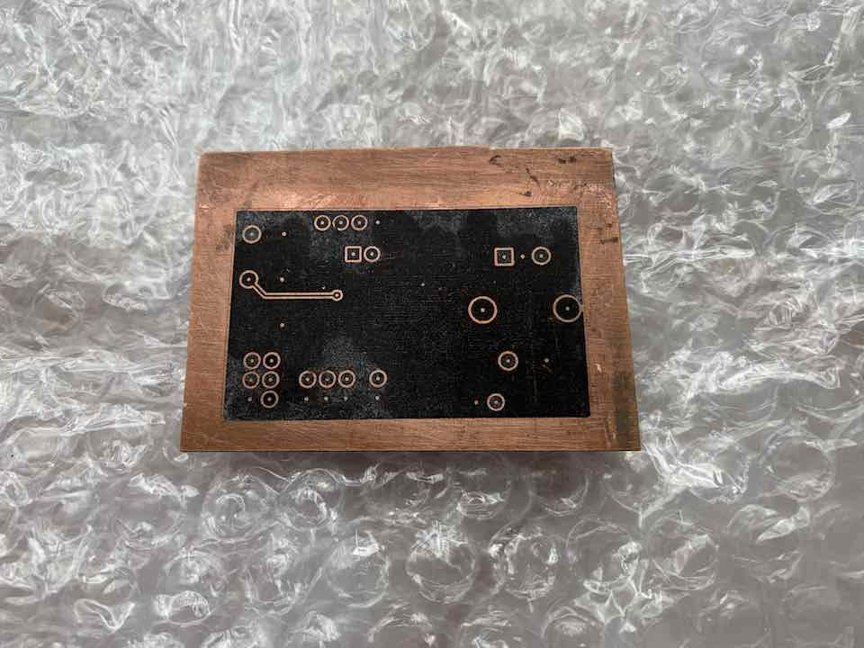
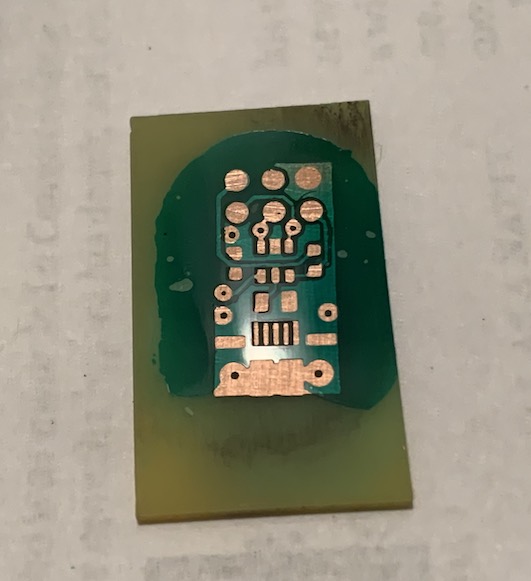
You can tell the board is done etching by shining a flashlight under it. Keep in mind not to leave the board in too long. When the copper next to a trace is gone, the etchant starts eating underneath it. Right when the large copper areas are gone is the perfect time to remove the board. Keep in mind that once you can see through parts of the board, it’s a good sign the board is almost done. Wipe off the toner with acetone. It should look a little something like this.
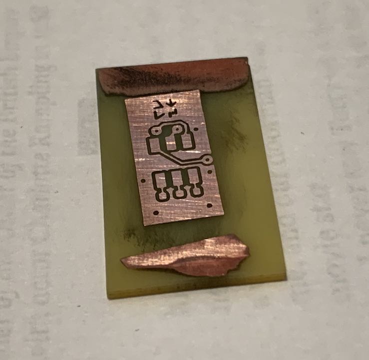
It’s a good idea to go under the microscope to double check that there’s no shorts or broken traces.
Soldermask
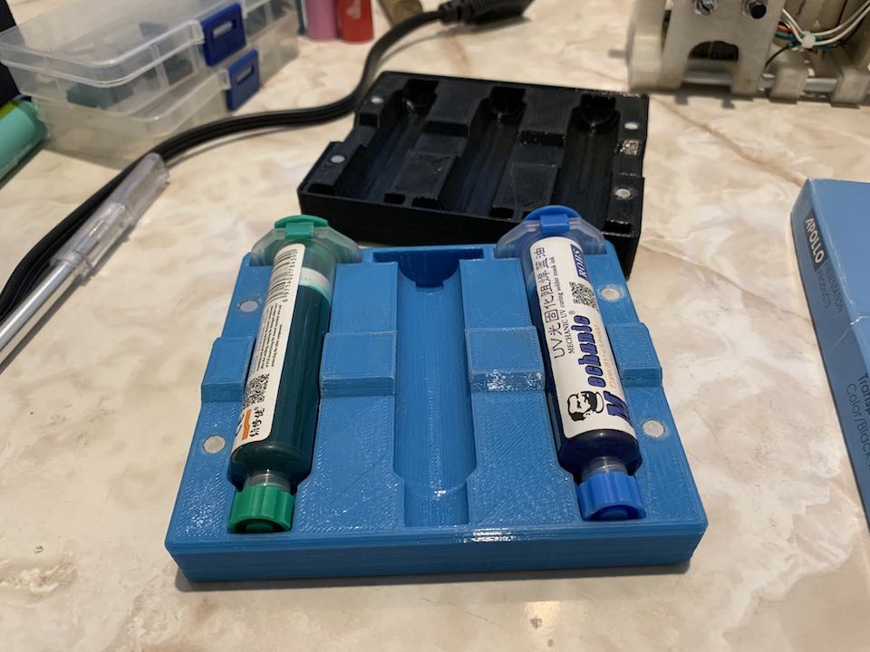
It can get a bit annoying when solder flows all over your copper traces, so soldermask is a really nice touch to add. I’m still perfecting my technique, but I have a general process that works pretty well. You’re gonna need some of that cheap UV curable soldermask you can get on eBay. Transparency sheets too. I have some old inkjet transparency sheets but they still work well in a laser printer. Start by printing the soldermask onto a transparency sheet. Cut it out and layer at least two of them together since the toner usually isn’t perfectly solid.
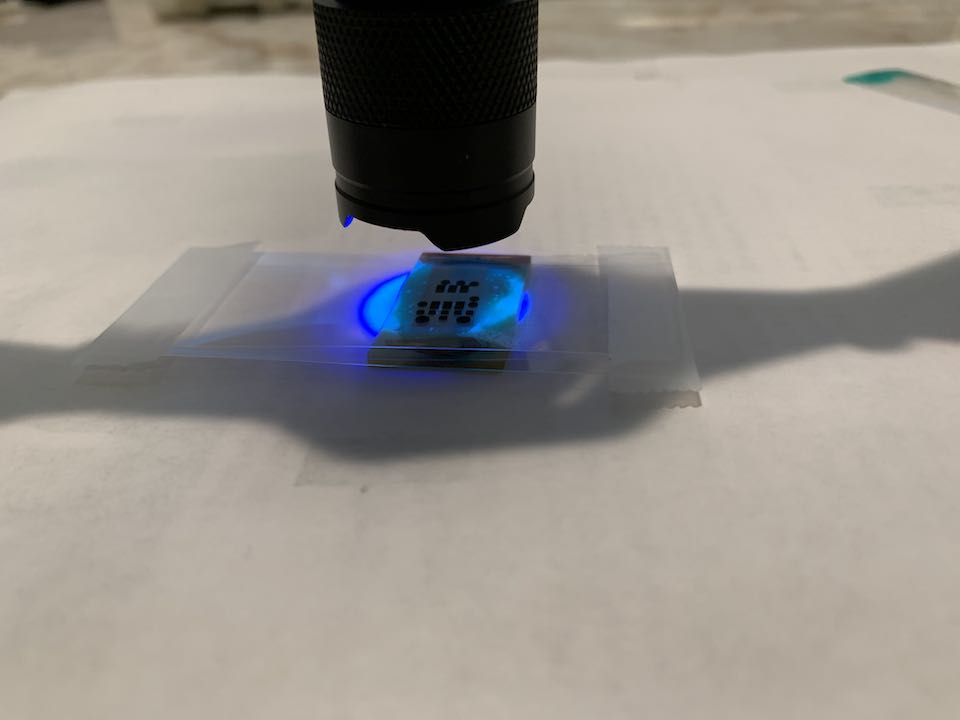
Now squeeze out some liquid soldermask onto your board and use some transparency sheet scraps to spread out a thin layer over the whole board. The thinner the better, but not to the point that there’s nothing there. Place your transparency with the soldermask pattern over it. I like to press down the transparency against the board with some acrylic. Now shine a UV light over your whole board. The flashlight I use works, but I think a stronger one would work better. I’m pretty sure sunlight works too but I tend to do things under the cover of night.
Cutouts and Drilling Holes
I like to drill holes after the soldermask because it’s annoying to clean out soldermask that flows into the holes. This is the most stressful part because of the human factor there’s much room for error. This is also the time to see how well aligned your vias are. There’s not much to say about drilling holes except make sure they’re aligned. You will end up breaking multiple drill bits so don’t worry too much.
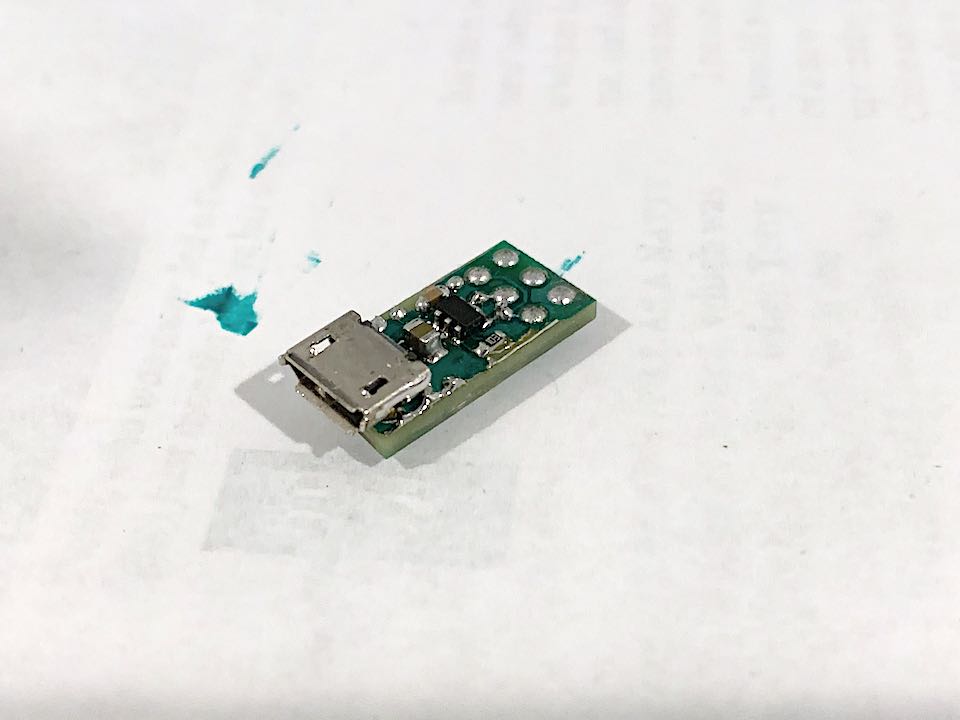
As for cutouts, I usually use a bandsaw to get the rough shape and then sandpaper the rest of the way. For really precise cuts like with my Nunchuk remote, I use a Dremel. One of these days I’ll incorporate my CNC mill back into this process to remove this human factor.
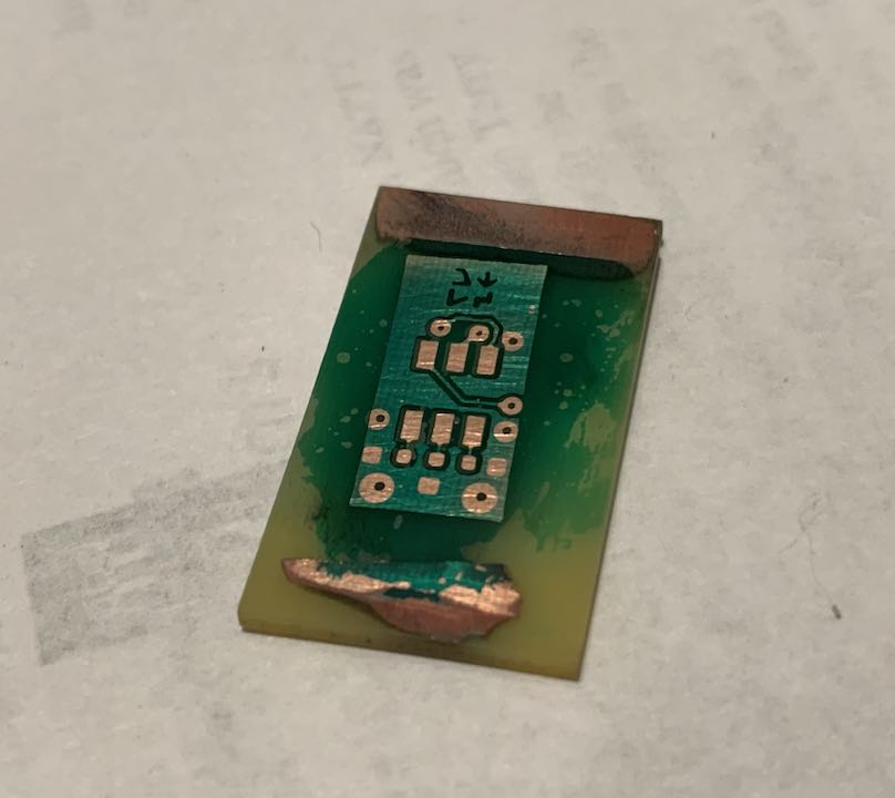
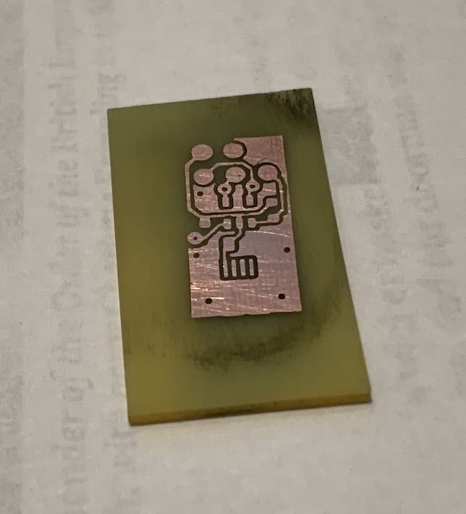
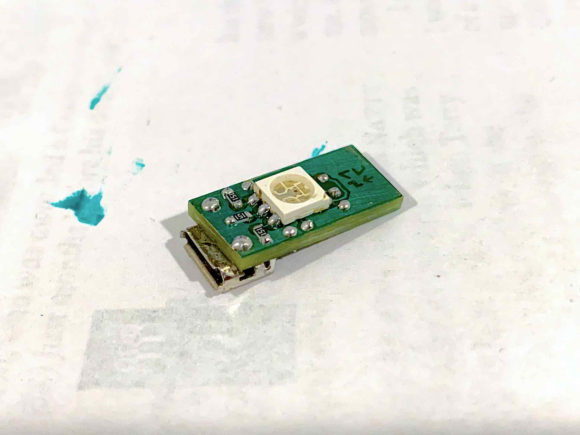
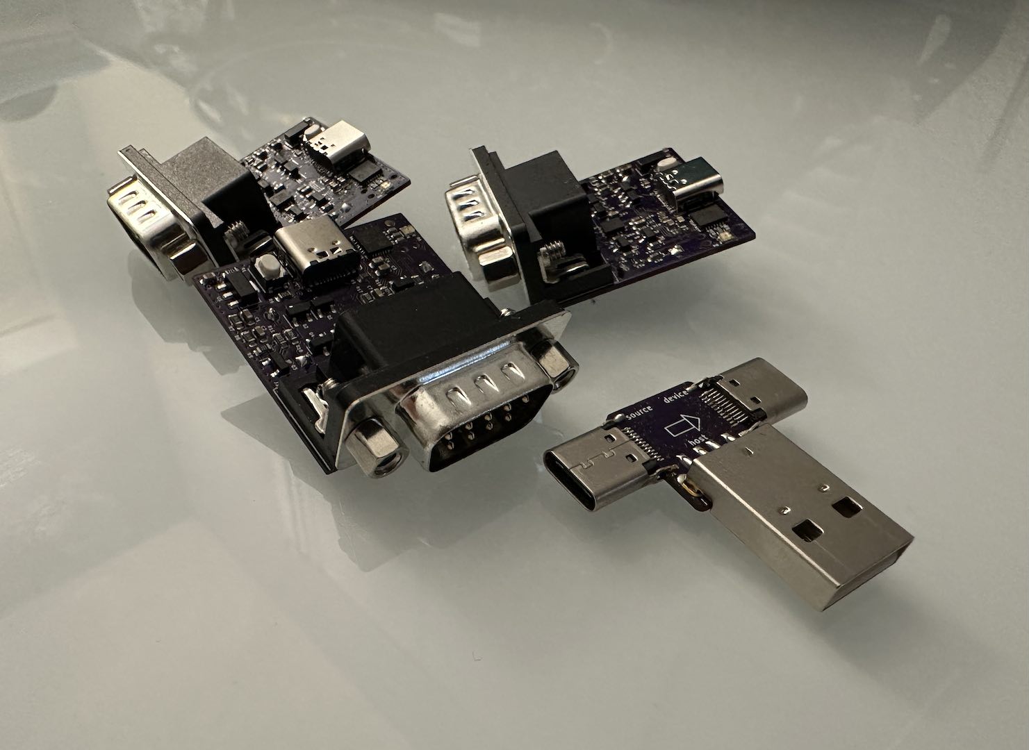
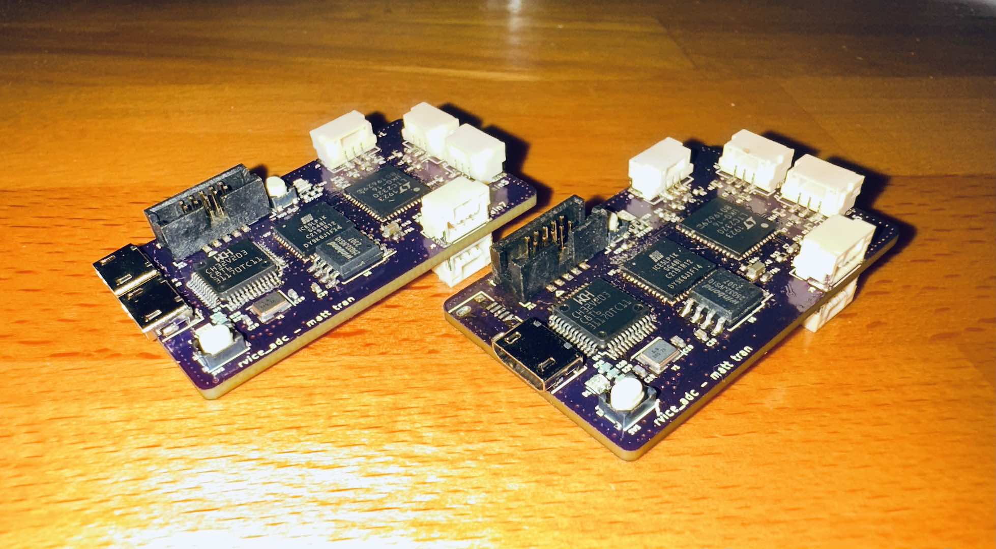
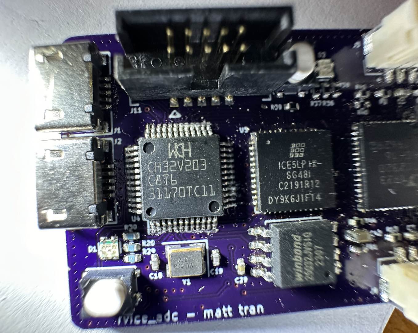
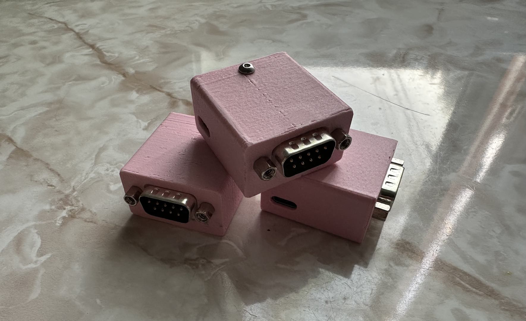
At the end of the day, you’ll end up with something like this.
Comments