
Custom Black Magic Probe
Continuing on the train of learning about ARM debuggers, I decided to take a look at one that I heard about for a long time and supported all the chips that I was interested in experimenting with next. However, the $60 price tag was a bit out of my budget. Since it’s an open source project, I took a look at the schematics and upon realizing it used an STM32F103 which I had some of, I decided to make one myself.
Design
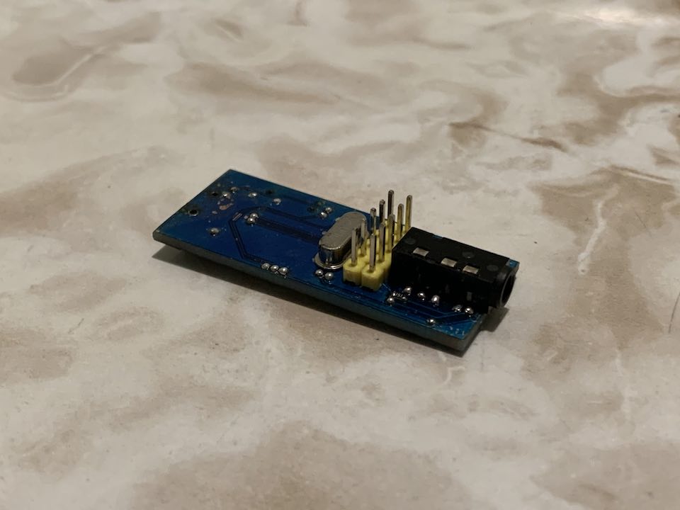
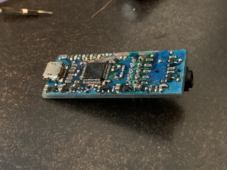
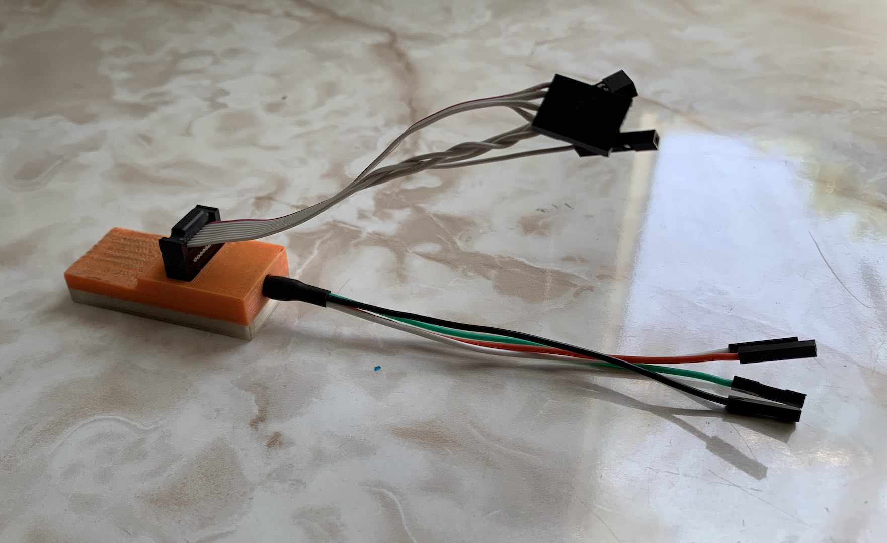
In order to keep the design compact and manufacturable with the limited components I had on hand, I changed a couple of things on the schematic. The USB TVS diodes and voltage translators were removed. The original design used a pair of P-channel MOSFETs to control target power, but I switched it out for an LDO instead. I connected the UART pins to a TRRS connector and added a Tag-Connect footprint for programming.
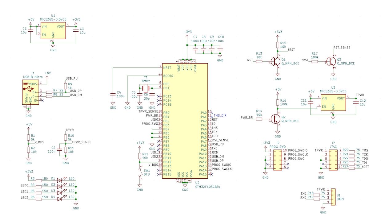
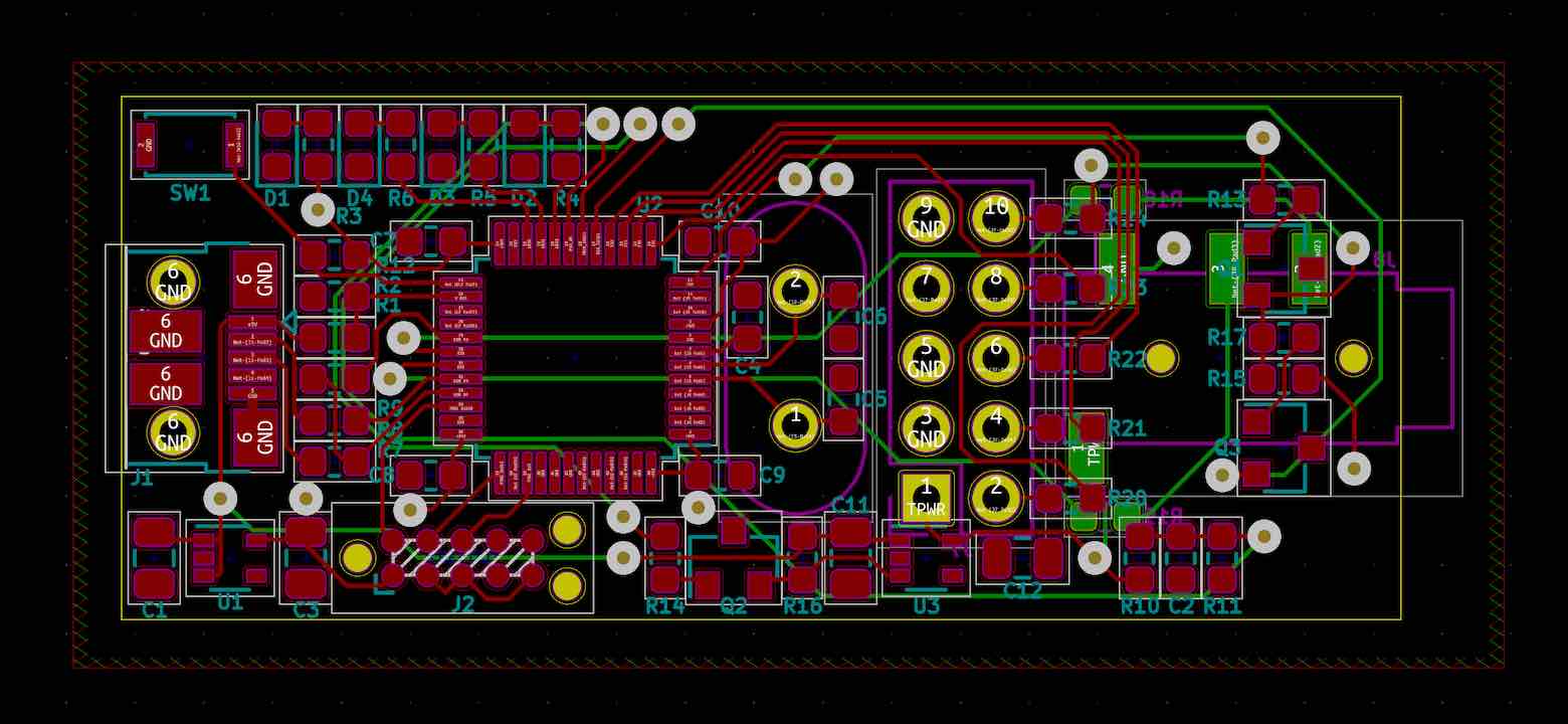
The PCB layout was relatively straightforward, but I had to use a 6.3 mil trace/space to keep everything small.
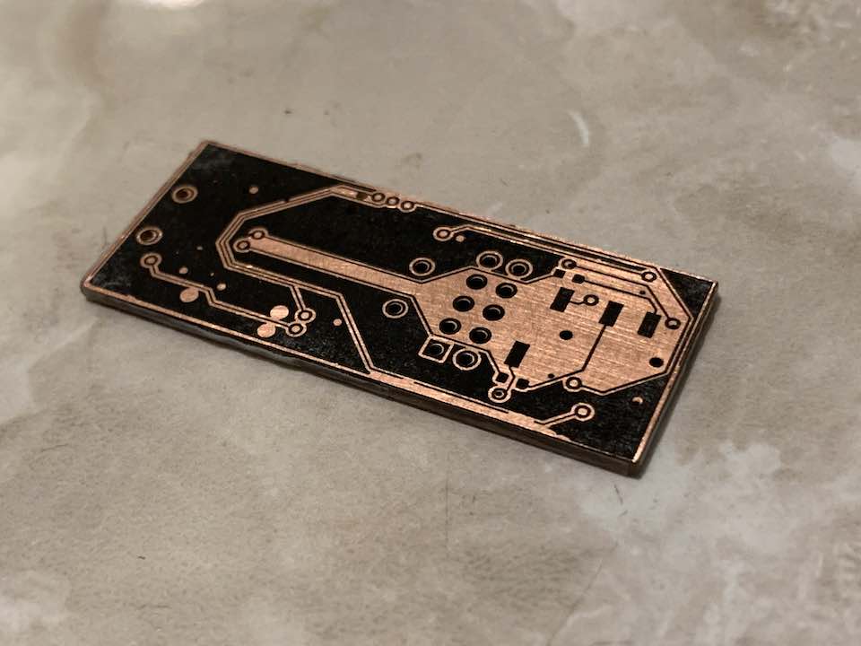
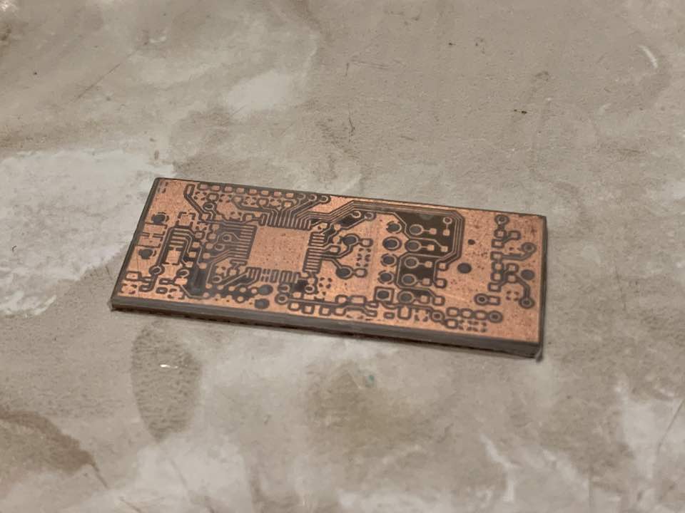
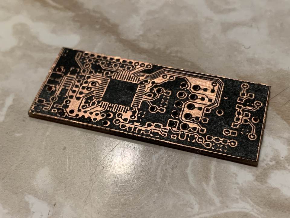
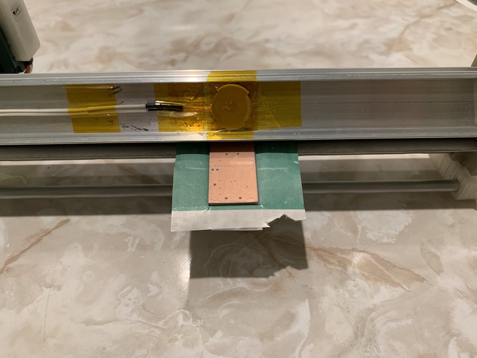
Manufacture
Manufacturing the PCB was the difficult part. To avoid drilling holes and cutting out the PCB manually, I brought out my CNC router to help me out. Since the PCB was now the exact correct size, I couldn’t tape on risers to etch both sides at once, so I did one at a time. Having one side face down also caused differences in etching rates so this improved overall quality. This was all back in April which was before I built my PCB agitator, so I’m surprised the traces actually came out mostly fine. Even the solder mask was decent considering I hadn’t developed my vastly improved technique yet.
Flashing
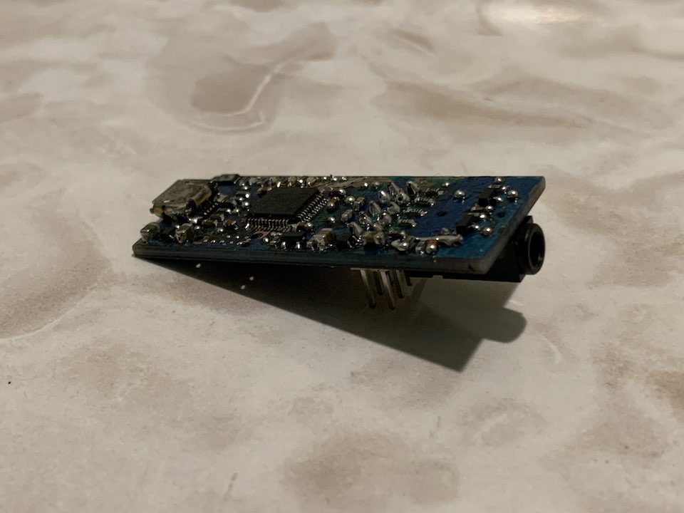
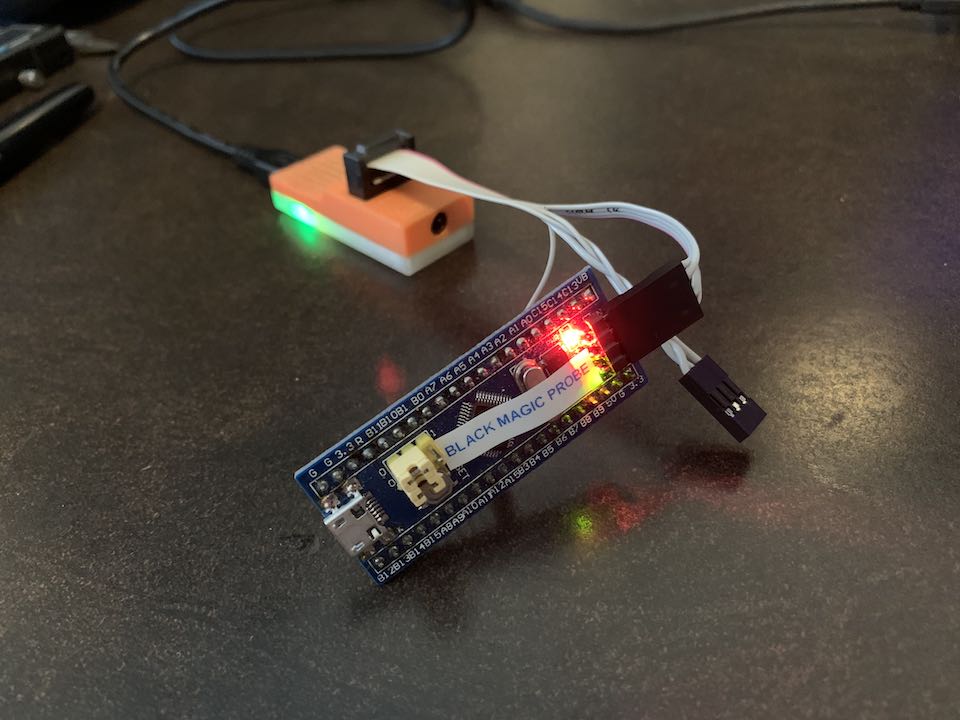
Flashing the BMP firmware onto the STM32 was tricky since I accidentally destroyed the programming pads while soldering. I had to solder some thin wires onto the LQFP package, but it worked out in the end.
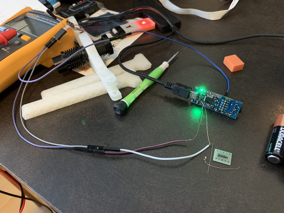
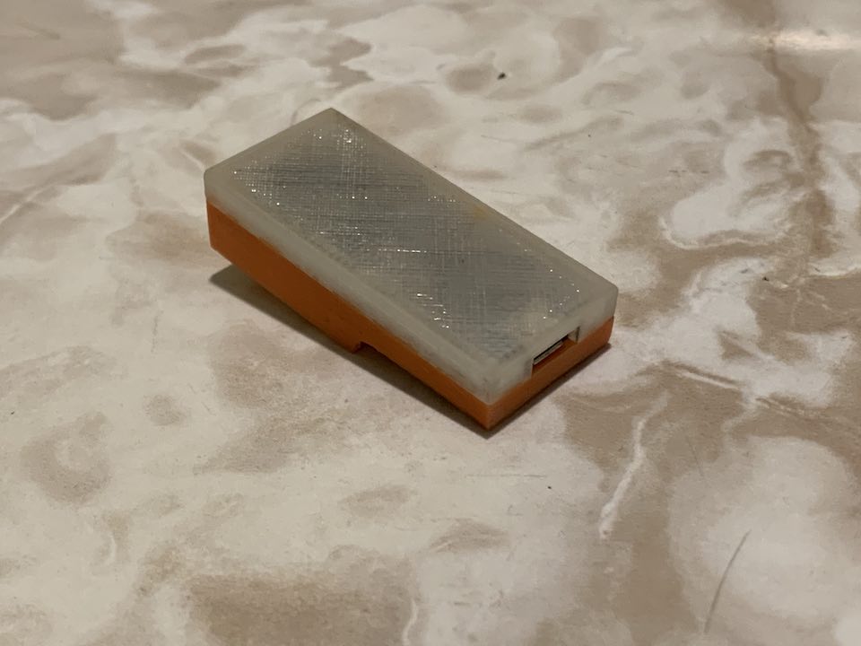
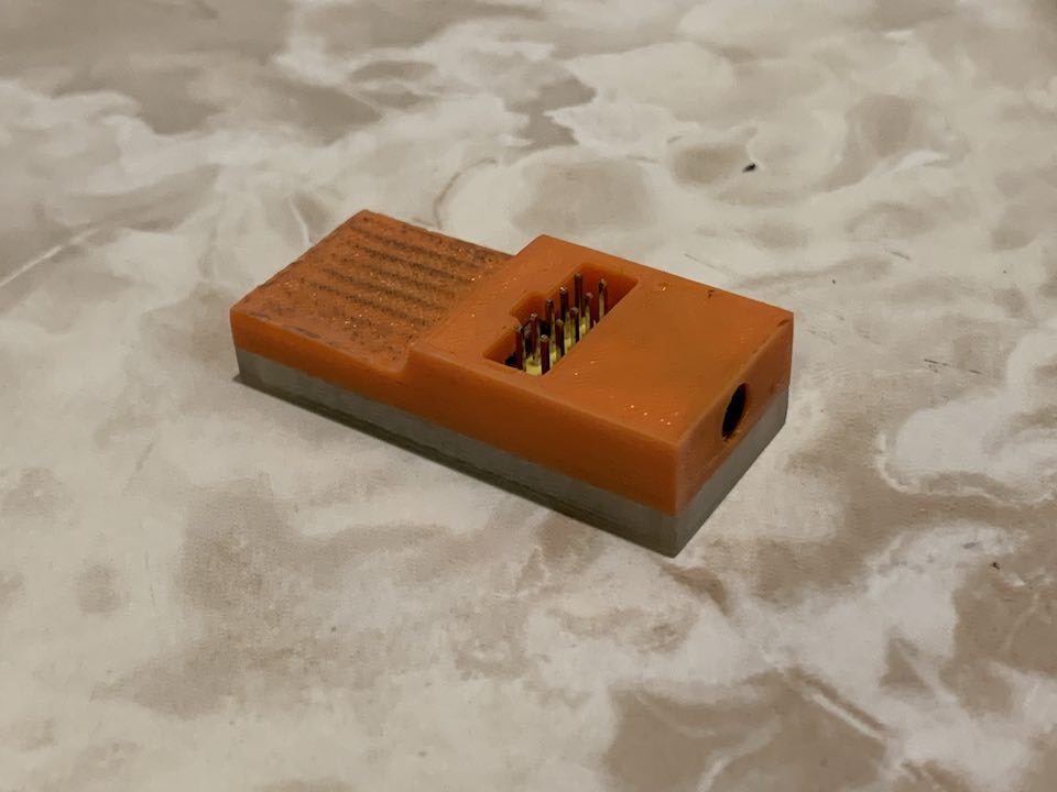
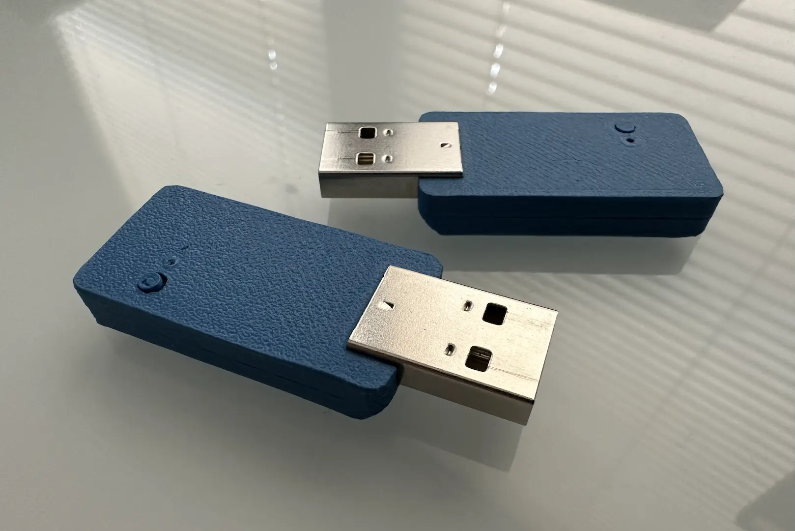
As always, I 3D-printed a case to protect the fragile PCB. I tried out JTAG for the first time and even programmed an ATSAMD21 breakout I made.

Comments