
RViCE ADC
https://github.com/dragonlock2/kicadboards/tree/main/projects/rvice_adc https://github.com/dragonlock2/miscboards/tree/main/lattice/rvice_adc https://github.com/dragonlock2/miscboards/tree/main/wch/rvice_adc
Looking through old parts in my stock, I came across the LTC2320 which I had samples of from years ago. Perusing the datasheet, it appeared that its protocol did not lend itself to a simple implementation on a microcontroller. Well, it does recommend using an FPGA. This was the perfect opportunity to build my first board that legitimately needed an FPGA. I also wanted to use a CH32V203 in something, so I had my project idea.
hardware
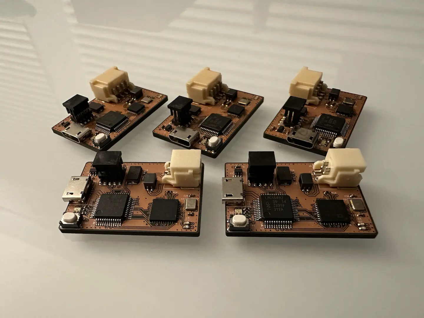
As always the hardware design was relatively simple. Just a matter of reading the datasheets and putting my blocks together. Due to the higher complexity, I organized everything into separate sheets. The ADC inputs needed anti-aliasing RC filters, which in hindsight need a cutoff frequency closer to 48kHz. I reused the power sequencing design from my Spartan 7 Breakout. The CH32V203 design was just like any other microcontroller. I used a bitbanged SPI to write to the flash chip and 2x SPIs for streaming ADC data from the FPGA. Looking back, I could probably come up with some sort of parallel interface using the GPIO to increase bandwidth. The iCE40 design was straightforward, but like the Spartan 7 took great care to ensure I wasn’t messing anything up. The LTC2320 ADC design was also straightforward and basically pulled straight from the datasheet.
As my first hardware design since March, I did a pretty good job especially with the layout and assembly. I used mostly 0402 components and a couple of 0603 capacitors that may or may not be smaller than recommended. Everything ended up fitting within two layers, even with the sheer number of nets connecting the chips. For assembly without a stencil, I used tweezers to pick and place tiny blobs of solder. By adding a minimal amount of paste across pads, not even on individual pads, I even got QFP soldered with almost no bridging.
software
Writing the firmware was really where the real complexity lies. This was also my first time using C++ in a more idiomatic way. I’ve documented the majority of my trials in Baremetal C/C++ on CH32V, but I’ll add more detail here. As always, I started by getting printf debugging working. Then I moved on to writing to the SPI flash. It took me way more hours than I’d like to admit to realize that the iCE40 was putting the SPI flash to sleep which explained why I didn’t get any responses to my commands. After fixing that, I added a very basic RPC over UART to test writing the flash via a Python script. Once that worked, I wrote some very basic Verilog built with the fully open-source Yosys toolchain to test the FPGA. Since UART is quite slow, I then moved the RPC to USB bulk transfers which brought the flashing time down to ~2s. Considering the synthesis time would be longer, this was fast enough. Interestingly, switching from C-style arrays to std::array and templates in the bitbanged SPI actually saved ~0.5KB of flash.
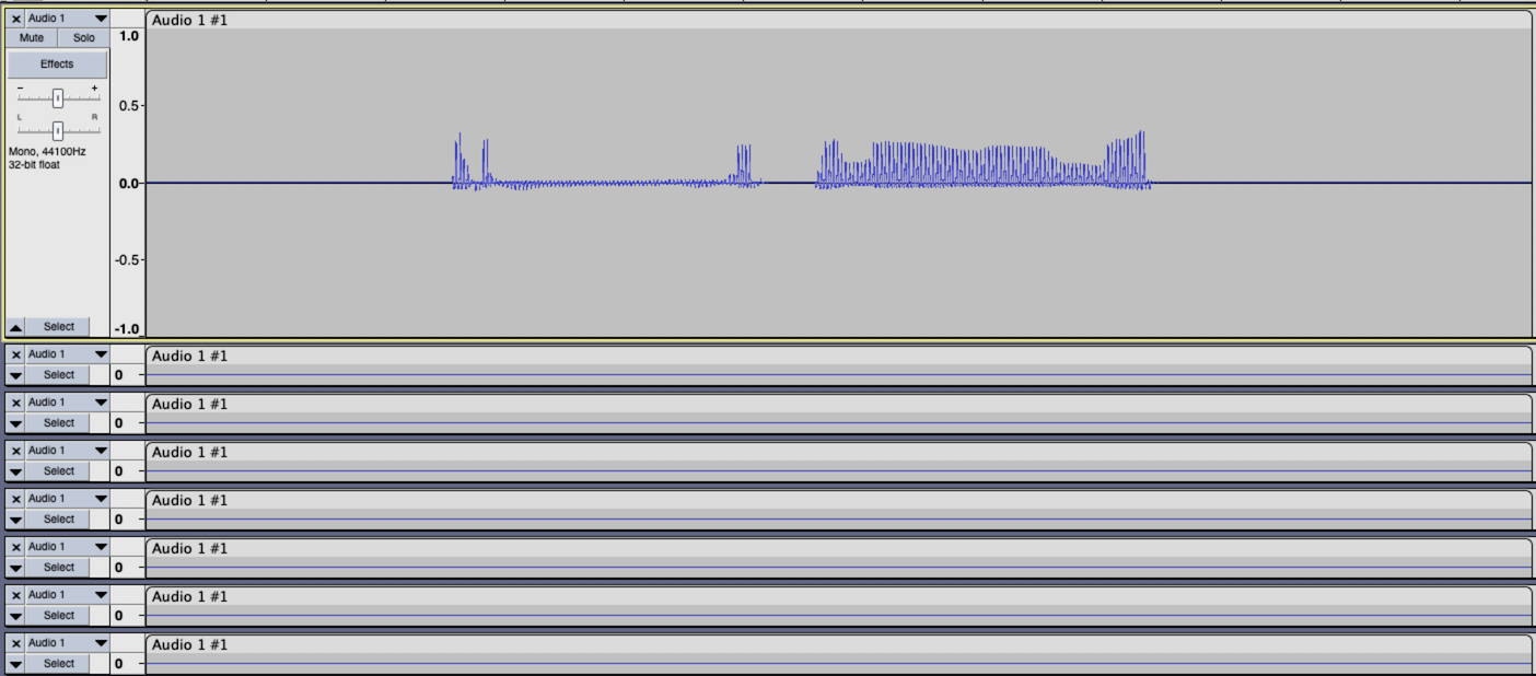
After that, I started working out how to get the ADC data out over USB. After learning about USB audio and doing the calculations, I realized I could get 8 channels of 48kHz, 16-bit data out over the USB FS connection. The ADC can do up to a 1.5MHz sample rate, but that would require USB HS and a lot more care on the FPGA side. TinyUSB provides decent audio examples, but getting the full 8 channels working was quite painful. It took a while to realize that isochronous endpoints do everything in one large packet without an ACK and then adding that support in my USB driver. It took a bit more time to realize that the FIFO buffer needs to ensure alignment of the channels, no partial channel writes, or else the OS could get confused and silently fail. After considerable effort and extensive use of Wireshark USB monitoring, I got it working.
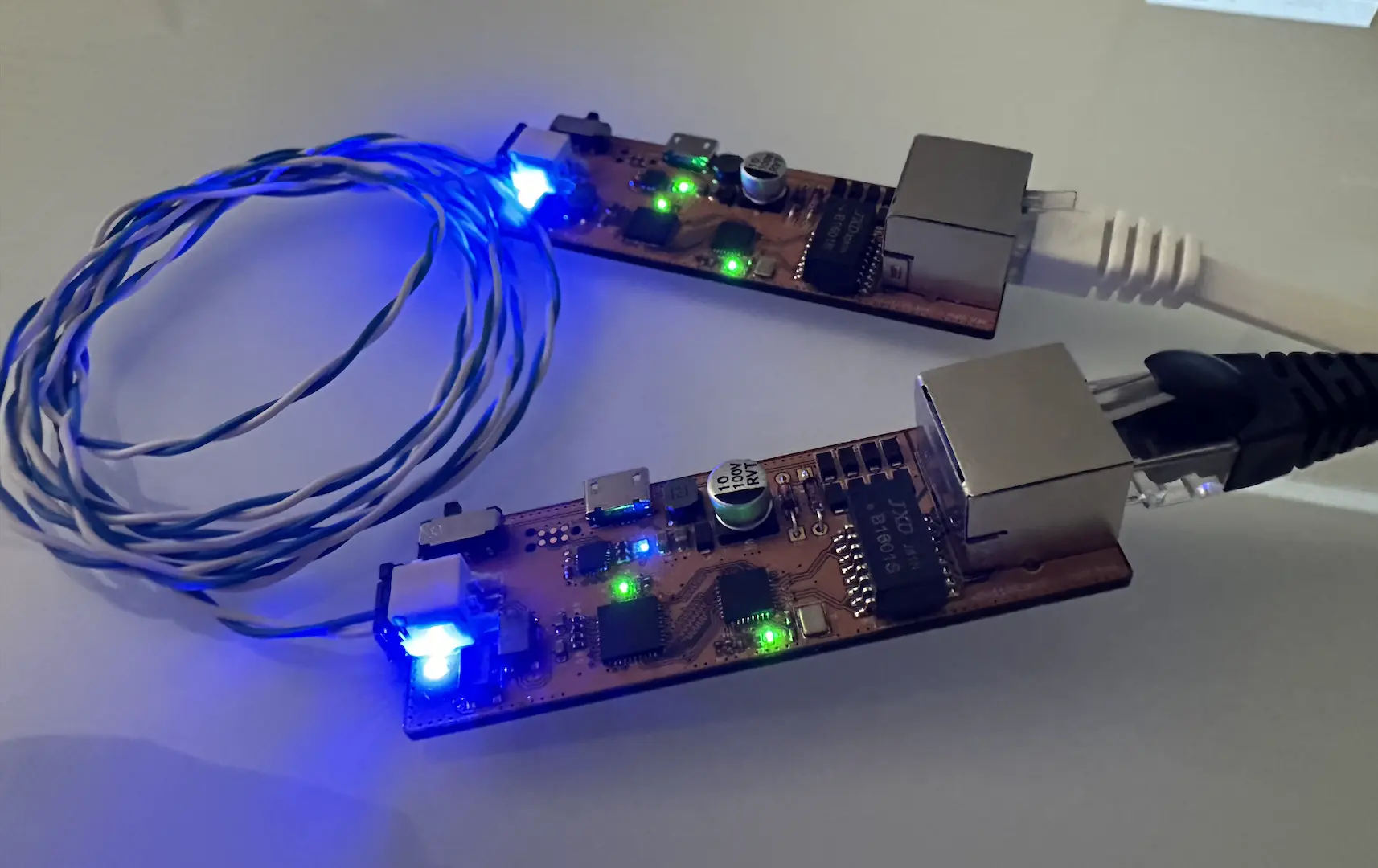
From there, I figured out how to get the ADC data off the FPGA. I designed in 2x SPI interfaces, but based on the bandwidth requirements I only needed one. Since the CH32V DMA doesn’t support variable strides, using only one also meant not needing to post-process buffers before sending out over USB or alternatively a much more complex Verilog implementation. One somewhat unnecessary worry was desynchronization between the microcontroller and FPGA SPI. What if it somehow ended up one bit off? To fix this, I had the FPGA assert on the CS line to signal that at least 1ms of samples was in its FIFO. At this point the SPI should be idle, so we can also resynchronize to the correct bit and sample boundary. Then the microcontroller would pull off 1ms worth of samples from the FIFO over SPI. During testing one annoying bug was that after flashing, samples could end up shifted one channel over. The samples were perfectly synced on an oscilloscope so I eventually realized this was caused by a DMA overrun where I started one before the prior one finished, leaving one sample in the SPI register that wasn’t easily discarded. Since my bitbanged SPI was in a critical section, this overrun made sense. The fix was simple, only start a DMA if the previous one finished.
Next, I worked on the Verilog for the FPGA. I would’ve used Chisel, but wanted to keep things simple. I started with PWM RGB and the PLL to get my feet wet. I ran it at 36MHz as it is an integer multiple of 48kHz. I didn’t realize the PLL doesn’t work below 10MHz and switched to a 72MHz clock from the microcontroller. Then I worked on the SPI which was difficult to sync because it had to work at 9MHz. Since the clock phases might not align, I had to add an input buffer on the clock to make things work. Due to that added delay, I actually shifted out the next data bit on the rising edge of the clock in order to get it physically shifting on the falling edge. After that, I added a very basic FIFO which was easy to implement. The one caveat was that iCE40 block RAM needs an extra clock cycle to read. From there, I worked on the ADC protocol. I used a state machine triggered by the 48kHz timer. The only bug I had to deal with was the samples coming in shifted. I was at home for the holidays without an oscilloscope, but eventually tracked it down to Yosys using 32-bit math on constants causing my CNV timing to be off. After that everything worked!
The LTC2320 is a pretty incredible part. Low noise, high resolution, high bandwidth. No wonder it’s nearly $40.

Comments